The capacity and energy efficiency challenges from the growing appetite for high-speed data along with advanced applications such as LIDAR and quantum computing are driving demand for increasingly large-scale photonic integrated circuits (PIC). With an ever-increasing number of components on a single photonic chip, manual techniques focused on the physical layout of components are becoming no longer feasible. In electronics, where circuits range to billions of transistors, the industry owes much of its success to standardized process design kit (PDK)-centric electronic design automation (EDA) workflows. Photonics, like electronics, needs reliable, scalable, and automated PDK-centric design flows as will be demonstrated in the upcoming webinar on June 28th, “Design a silicon photonic ring-based WDM transceiver with EPDA”.
Automated generation of foundry compatible compact model libraries
In electronics, IC designers focus on their gate-level simulations without worrying about the in-depth complexities at the transistor level or process compatibility of the actual physical implementation. This separation of the logic-level design frees IC designers to focus on high-level functionality and is mainly enabled thanks to reliable and consistent software tool chains that break down the complexities of large-scale system design via multiple layers of abstraction, as well as the availability of accurate model libraries provided in foundry PDKs. Photonics has been evolving along the same lines to enable scalable design from concept to a working photonic chip.
In the device-level simulation, the physical geometry of the materials is defined, and its effects are simulated in multiple physical domains via compute-intensive solvers. These computationally demanding simulation methods at the component level are not feasible for addressing entire photonic circuits or even single devices with large geometries. To address photonic design on a large scale, abstract design methods are needed. Like the electronics industry, photonic devices at the component level are abstracted into compact models and represented as blocks that can be connected in a schematic design environment to create specific functionalities. Each building block has input and output ports with a defined behavioral response both in time and frequency domains. Today most advanced PIC designers start with a schematic that captures the targeted functionality of the overall system in terms of smaller, hierarchical compact models. The accuracy of a circuit simulation is dependent on the accuracy of the models in its building blocks which are defined based on component-level simulations, measurements from device characterization, or a combination of both.
Accurate models not only need to capture the complex interplay of underlying multiphysics effects in photonic devices but also must be manufacturable at a high yield. After all, yield is what makes a design commercially viable. Process variation is inherent to manufacturing and includes statistical correlations of individual circuit elements in addition to spatially dependent variability, all of which can significantly impact the performance of individual devices and the overall circuit. Statistical models are needed for yield analysis to account for process variability and ensure that the designs will behave as intended after fabrication.
To successfully create such models, designers require seamless multiphysics simulation workflows that enable optimization of custom components with built-in capabilities to account for manufacturing variability and ensure compatibility with a foundry process. Even with access to comprehensive multiphysics solvers and yield analysis capabilities, enabling PIC design in the face of lacking standards around the generation of compact model libraries (CMLs) is still extremely challenging. Without standards, deciding what equations and parameters to use for encapsulating all the relevant phenomena of each component into its respective compact model can be a daunting task. Additionally, circuit designers want access to varying versions of foundry-specific CMLs that cover a large set of comprehensive and parametrized device models. Manually generating and maintaining such libraries is an extremely challenging, cumbersome, and error-prone process that hinders engineering productivity and simply does not scale. Ansys’ Lumerical suite of products enables comprehensive multiphysics simulation of photonic components, accurate time and frequency domain simulation of PICs, automated generation of statistical photonic CMLs as well as yield analysis which in turn enable standardization of a PDK centric design flow.
Schematic-driven flows for co-designing electro-photonic circuits
The design workflow discussed so far describes how multiple optical functionalities can be combined to create photonic circuits. In real designs, photonic circuits are connected to electronic circuits and it’s their combined functionality and performance that must be optimized. Circuit simulators in electronics model signal as voltages and currents, but there are unique requirements for photonic circuit simulation methods. Optical signals carry both amplitude and phase, have a wavelength, and are bi-directional and multi-mode in nature. Photonic circuit simulators must capture all these phenomena.
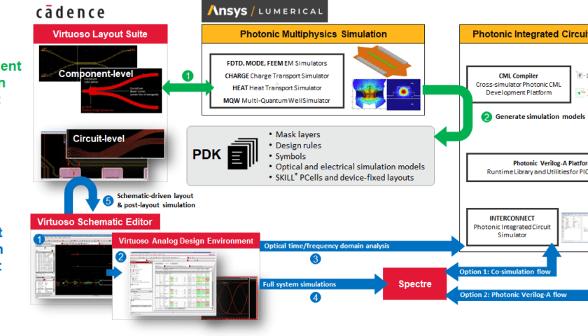
On the layout side, unlike the Manhattan shapes in electronics, photonic designs require support for curvilinear geometries which also creates complex design rule checking (DRC) and layout versus schematic (LVS) challenges. Ansys Lumerical and Cadence jointly developed state-of-the-art electronic-photonic design automation (EPDA) solutions that use best-in-class photonic and electronic tools to eliminate the design scaling limitations both in the front-end and in the back end of the design flow.

An overview of the EPDA design flow is depicted in the figure
PICs include many active optoelectronic blocks such as lasers, photodetectors, and modulators that have associated electronic drivers and tunning circuits. Co-simulation of the electronic and photonic circuits captures the tight interactions between the optical and electrical domains. Consider the electrical feedback loop comprised of monitoring photodetectors and associated TIA sub-circuits used in tuning the resonant wavelength of modulators in a ring-based transceiver design. Even though this use case doesn’t necessarily require a high-speed feedback loop, there is still continuous interaction between the detection and the tuning blocks and, given the multi-channel topologies of transceiver designs, designers would need to keep track of millions of data points being exchanged between optical and electrical circuit simulators. You can learn about building compact models, curvilinear photonic layout, co-design, co-simulation, and schematic-driven layout with back-annotation in our upcoming webinar on June 28th Design a silicon photonic ring-based WDM transceiver with EPDA.
For more detail please visit easybom


Discussion about this post